Growth and Surface Engineering of Nanowires for Optoelectronic Applications and the Unfolding Discoveries of the Physics of Light
- 16 Jun 2017
- Volume 7
- NanoScientific Magazine, Summer 2016

Physics Department, Max -Planck Institute for the Science of Light Photonic Nanostructures Group, Germany
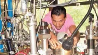
Since 2012, Dr. Muhammad Y. Bashouti has been principle investigator at the research group 'Photonic Nanostructures' headed by Prof. Silke Christiansen in the Division of Prof. Dr. Gerd Leuchs at the Max-Planck Institute for the Science of Light, (MPL). Bashouti received his bachelor degree in chemistry at the Hebrew University/Israel and completed his Ph.D. in physical chemistry at Technion-Israel Institute of Technology (IIT). He has published more than 35 papers in peer-reviewed publications, is an editorial board member of several scientific and received numerous awards. The Max Planck Institute for the Science of Light performs basic research in optical metrology, optical communication, new optical materials, plasmonics and nanophotonics and optical applications in biology and medicine. The Institute founded in 2009 is based on the Max Planck Research Group "Optics, Information and Photonics". The Max Planck Society consists of 83 research institutes with over 13,300 employees who are doctoral students, postdoctoral students, research fellows and visiting scientists. The Max Planck Research Institutes are divided into three categories: Biology & Medicine, Chemistry, Physics and Technology and Human Science. The Max Planck Society was voted best employer in the natural sciences for three consecutive years and is part of a diverse international partnership with affiliates in Canada, USA, Spain, Israel, India, Korea, Japan, France and Switzerland. The Max Planck Institute for the Science of Light (MPL) was founded in January 2009, making it one of the youngest Max Planck Institutes. It consists of three divisions, several independent research groups and three technical development and service units (TDSU).
ARE A PROMISING CANDIDATE FOR THE REALIZATION OF HIGHLY INTEGRATED ELECTRONIC, PHOTONIC AND OPTOELECTRONIC DEVICES AS WELL AS FOR FUNDAMENTAL STUDIES IN NATURAL SCIENCES.
What is the science of light and what can we learn about it to apply to new technologies?
The science of light at our group at Max Planck at Erlangen focuses on research fields that are particularly innovative or especially demanding in terms of funding or time requirements. In particular; our interest is somewhere between basic research and technology development with a focus on the photonic nanostructures for various applications in the areas of opto-, nano- and large area electronics, optical and electrical sensing as well as nano-photonics. This implies the synthesis, building and structuring of novel nano- and nanocomposite materials together with their characterization and modeling. This work covers a wealth of different scientific disciplines ranging from condensed matter physics, semiconductor and theoretical physics over physical and organic chemistry to engineering disciplines like electrical and mechanical engineering as well as material science. It is important to mention that that group is leaded by Prof. Dr. Silke Christiansen who is the Director of the Institute of Nano-architectures for Energy Conversion at the Helmholtz-Center for Materials and Energy at Berlin as well.
What is photonic nanomaterials and how is it useful in society?
Photonics nanomaterial can be defined by the combination of “photonic” and “nanomaterial” which is the interaction of light (photon) generation, detection, and manipulation (through emission, transmission) with nanomaterials. Thus, many classes of materials such metamaterials, photonic crystals, plasmonics, diffractive structures can be included. Photonic nanomaterials with efficient optical (or electrical) transfer while keeping standards, belong to the biggest challenges of mankind in the 21 century. Our proposed sciences and technology will have an important impact on future technology and ultimately on our daily life. By answering the scientific and technological questions that we have addressed to ourselves, new innovation and developing devices will be revealed and will be done. Fast data transfer, high capacity storage at the level of a few nanometers, and saving energy are examples for the impact of the research between light and matter.
Why Semiconducting Nanowires?
Given the demand for ever more compressed and fast systems, there is growing interest in the development of nano-devices which enable new functionality and enhance performance. Over the last 50 years, the scaling of silicon-based electronics shifted to ever smaller dimensions and the focus of device design mechanisms changed from bulk to surface and interface properties which became significantly more important. With the progress in nanomaterial fabrication, Silicon nanowire (Si NW), in particular, a wealth of novel nano-device concepts were developed. A legitimate question is: what makes a silicon nanowire different from bulk systems? The answer is mainly to the credible platform on which to build the next generation of optoelectronic devices. They are always semiconducting, because of their aspect ratio they can be simultaneously used as the active region of the device, e.g. the channel of a field-effect transistor, or to connect different devices, the ability to manipulate their properties through controlling their surfaces (by molecules for example), and – most importantly – they can be naturally integrated within the existing Si-based nanotechnology.
What are solar cell based silicon nanowires and why are they important?
Solar cells based aligned Si NW arrays can bare the potential for efficiencies >15%. They can be fabricated on single or multi -crystalline silicon (mc-Si) layers on Si wafer or glass respectively. They can be realized through top down approach such as reactive ion etching (RIE) with lithographic large area nano patterning using densely packed polystyrene (PS) spheres. Geometrical parameters such as diameter, length, density and shape of SiNWs can be tuned for highest absorptions (close to 90%). Various SiNW solar cell concepts are presented: (i) a hybrid organic/inorganic cell with SiNW -based absorber and a hole conducting polymer (PEDOT:PSS - encapsulation procedures for long term stability suggested); (ii) a semiconductor -insulator -semiconductor (SIS) cell with SiNW absorber, oxide (few angstroms Al2O3 by atomic layer deposition -ALD) ) tunneling barriers for charge carrier separation and a transparent conductive oxide (TCO – here: Al:ZnO, by ALD). Initial thin film solar cell prototypes reached open -circuit voltages of > 630 mV, short -circuit current densities of even ~ 30 mA/cm 2 and efficiencies >13%.
“THE SCIENCE OF LIGHT AT OUR GROUP AT MAX PLANCK AT ERLANGEN FOCUSES ON RESEARCH FIELDS THAT ARE PARTICULARLY INNOVATIVE OR ESPECIALLY DEMANDING IN TERMS OF FUNDING OR TIME REQUIREMENTS. IN PARTICULAR; OUR INTEREST IS SOMEWHERE BETWEEN BASIC RESEARCH AND TECHNOLOGY DEVELOPMENT WITH A FOCUS ON THE PHOTONIC NANOSTRUCTURES FOR VARIOUS APPLICATIONS IN THE AREAS OF OPTO-, NANO- AND LARGE AREA ELECTRONICS, OPTICAL AND ELECTRICAL SENSING AS WELL AS NANO-PHOTONICS.”
What is optoelectronic characterization and how is it done?
Correlated microscopies / spectroscopies are used to improve materials / cells: (i) electron beam induced current (EBIC) – to study charge carrier distributions in nano -architectures; (ii) electron backscatter diffraction (EBSD) – to study structural quality of the multi -crystalline Si layer before and after patterning; (iii) integrating sphere measurements, external quantum efficiency, photo - and cathode -luminescence – to study optical properties and (iv) 4 -point nano -probing of individual NWs – to study electrical properties. Novel electrodes (e.g. graphene, silver nanowire webs) to further improve the cells are evaluated.
Why is it important to understand surface properties and which equipment is used to measure surface properties?
The large surface area per unit volume of nano-materials makes them highly sensitive to surface characteristics such as surface morphology, topography and physical/chemicalbonds with otheratoms and molecules. Indeed, the terminationof surface dangling bonds with chemical and or biochemicalmoieties is expected to have a significant impact on the final physical and chemical properties of the nanomaterials (such as nanowires). Therefore, Si NW based composites can be scaled down to the molecular level by applying surface functionalization, which cover the NW surfaces with molecules bonded to individual surface atoms.The resulting Si NWs are known as “hybrid-Si NWs”. For example, a large body of chemistry has been developed for linking moieties chemically to oxidized Si NW surfaces, generally through -OH chemistry, and to oxide free silicon through Si-C bonds. It is therefore essential to understand the surface properties and charge exchange between the NW surfaces and their bulk on a microscopic level. The main analytical tool adopted in surface science is photoelectron spectroscopy and kelvin probe. Band diagrams will be extracted based on this analysis and correlated with electrical and material properties of the NWs.
With so much discussion about light, can you tell us what Dark Matter andDark Energy are and what does that tell us about the universe?
The interaction between light and matter gives a lot of information about our surrounding. Since the first pioneer discovery of Hasan Ibn al-Haytham(Alhazen)regards real matters at the 10th century, the field of optics get a great light spot from the researchers and a new hypothetical matters were suggested such as Dark Matter. Generally speaking, dark matter is a term used in astronomy and cosmology to describe matter that is undetectable by its emitted radiation, but whose presence can be inferred from gravitational effects on visible matter and composed of baryons, i.e. protons and neutrons. Interestingly enough, at 1998,the NASA scientists’ observed with the help of Hubble Space Telescope (HST)that the Universe was actually expanding more slowly than it is today. So the expansion of the Universe has not been slowing due to gravity, as everyone thought, it has been accelerating. Theorists still don't know what the correct explanation is, but they have given the solution a name and called it “dark energy”.

What is white light and how can it be used in our society in the future?
Saving energy is crucial for the mankind nowadays. Bright and white light sources are considered as an energy-saving and are necessary for humanity in many disciplines such as housing, roads, etc. Thus, the great work of Shuji Nakamura, one of the three recipients of the 2014 Nobel Prize for Physics was regarded as the inventor of the blue LED, a major breakthrough in lighting technology. Together with Isamu Akasaki and Hiroshi Amano, they own the prize for the invention of efficient blue light-emitting diodes, which has enabled bright and energy-saving white light sources. This is an example for the importance of the science contribution for society and impact of light related material physics understanding.
How is Mobius strip and polarization of light helping scientist study light and particles?
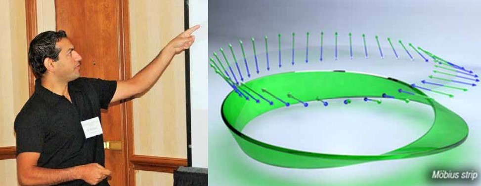
Möbius strips are simply a three dimensional structure that has only one side. It’s very simple to create, for example, twisting a piece of paper gives you the Möbius strip shape. The Möbius strip created from the polarization of lightand opens up new possibilities for material processing and for and nanotechnology and confirming a light's electromagnetic fieldtheoretical prediction.
What are the most interesting new findings at the Max Plank Institute that is currently expanding our understanding of our world?
I think the best answer to deliver is to continue discussion the pervious question.The Möbius strip generated from laser light by scientists from the Max Planck Institute for the Science of Light (our director Prof. Dr. GerdLeuchs) and FriedrichAlexander-Universität Erlangen-Nürnberg (FAU), among others, could be the appropriate optical tool to produce the corresponding nano-scopic structures from a material. I suggest to contact him for further information.
“INTERESTINGLY ENOUGH, IN 1998, NASA SCIENTISTS OBSERVED WITH THE HELP OF THE HUBBLE SPACE TELESCOPE (HST) THAT THE UNIVERSE WAS ACTUALLY EXPANDING MORE SLOWLY THAN IT IS TODAY. SO THE EXPANSION OF THE UNIVERSE HAS NOT BEEN SLOWING DUE TO GRAVITY, AS EVERYONE THOUGHT, IT HAS BEEN ACCELERATING. THEORISTS STILL DON'T KNOW WHAT THE CORRECT EXPLANATION IS, BUT THEY HAVE GIVEN THE SOLUTION A NAME AND CALLED IT DARK ENERGY.” "I HAVE USED ATOMIC FORCE MICROSCOPE (AFM) IN MY RESEARCH BECAUSE IT IS VERY USEFUL IN MAPPING THE SURFACE, ROUGHNESS AND TOPOGRAPHY AND I ALSO PLAN ON USING AFM ON MY NEXT PROJECT"

Dr. Muhammad Y. Bashouti,
Department Of Physics, Max Planck Institute For The Science Of Light
