Park Systems Opens Nanoscience Center at SUNY Polytechnic Institute
- 11 Feb 2018
- Volume 12
- NanoScientific Magazine, Winter 2018
The Park Nanoscience Center in Albany, NY is a new branch of Park Systems and will showcase advanced atomic force microscopy (AFM) systems, demonstrate a wide variety of cutting-edge applications—ranging from materials science, to chemistry and biology, to semiconductor and data storage devices— and provide hands on experience, training and service, year-round.

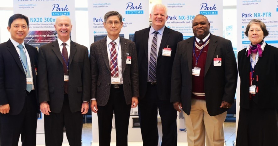
Pictured (left to right): Dr. Ryan Yoo, Vice President of Sales at Park Systems, Mr. Keibock Lee, President and General Manager at Park Systems, Dr. Sang-il Park Chairman & CEO from Park Systems, Prof. Alain Diebold, Interim Dean at the College of Nanoscale Science at SUNY Polytechnic Institute, Dr. Ardavan Zandiatashbar, Technical Accounts Manager and Sr. Applications Scientist at Park Systems
The Center’s grand opening at the State University of New York Polytechnic Institute (SUNY Poly), one of the world’s most advanced high-tech education, research and development sites, was held on November 10, 2017 at 2 PM. The Center is located in the NanoFab East Building of SUNY Poly’s Albany campus and is designed to become a hub for globally advanced metrology AFM research activities. It will be equipped with the latest Park AFM systems, including the Park NX20, Park NX10, and Park NX-Hivac. Park Systems, a global AFM manufacturer, has offices in key cities worldwide, including Santa Clara, California; Tokyo, Japan; Singapore; Heidelberg, Germany; and Suwon and Seoul, South Korea.
SUNY Poly’s Albany NanoTech Complex is home to the College of Nanoscale Sciences and the College of Nanoscale Engineering and Technology Innovation and is a fully-integrated research, development, prototyping, and educational facility that provides strategic support through outreach, technology acceleration, business incubation, pilot prototyping, and test-based integration support for onsite corporate partners, including IBM, GlobalFoundries, Samsung, TSMC, Applied Materials, Tokyo Electron, ASML, and Lam Research, as well as other next-generation nanotechnologybased research activities.
“As SUNY Polytechnic Institute provides cutting-edge educational and research and development opportunities, it is exciting that Park Systems will establish operations at our Albany campus,” said Dr. Alain Diebold, SUNY Poly Interim Dean of the College of Nanoscale Sciences; Empire Innovation Professor of Nanoscale Science; and Executive Director, Center for Nanoscale Metrology. “Our scientists and engineers look forward to working closely with Park Systems to enhance next-generation technologies that will lead to improved metrology capabilities for researchers and members of industry around the world.”

“SUNY POLY IS THRILLED THAT A WORLDWIDE LEADER IN ATOMIC FORCE MICROSCOPY IS SELECTING THE CAMPUS FOR ITS NEWEST LOCATION, AND WE WARMLY WELCOME PARK SYSTEMS AS WE LOOK FORWARD TO WORKING CLOSELY TO ADVANCE RESEARCH CAPABILITIES IN THIS IMPORTANT AREA,"
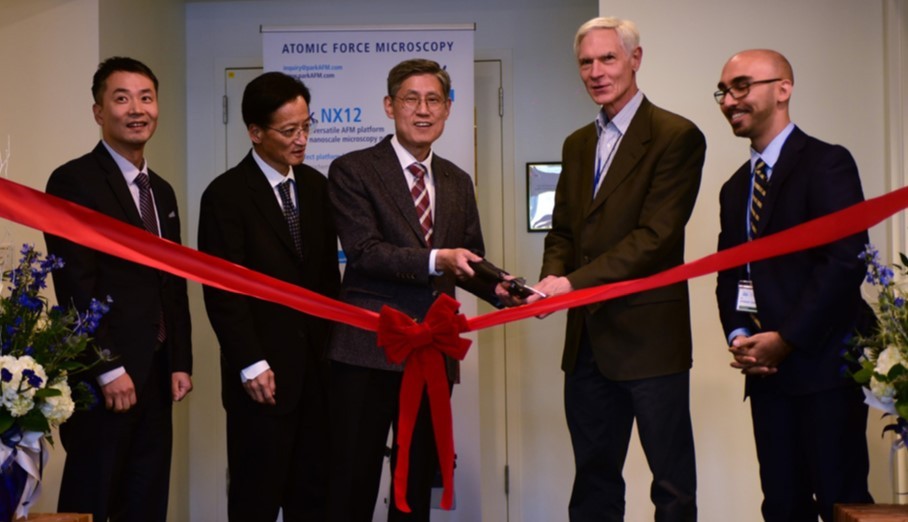
Park Nanoscience Center Grand Opening Event
In his opening remarks at the ceremony Dr. Sang-il Park, Park Systems Chairman & CEO, highlighted Park Systems’ continued growth and success as the world leading atomic force microscope manufacturer for over two decades. This year marks the 20th anniversary for Park Systems and in 2015 the company went public, becoming the only successful public offering for an AFM business. Since the IPO, their stock has increased by 168% and many companywide growth initiatives have set the platform for continued future success. Park’s recent accomplishments include expansion of their Korean facility and the creation of a new advanced cleanroom. They also opened offices in Taiwan, Germany, and Singapore, and added key personnel for global expansion. The opening of the Park Nanoscience Center at SUNY Polytechnic Institute adds Park Systems to a prestigious list of material suppliers, equipment suppliers, and IC manufacturers at that location. SUNY Polytechnic is a very semiconductorcentric site. “We have a national treasure here in terms of a robust ecosystem for semiconductor research,” commented Dr. Alain Diebold, SUNY Poly Interim Dean of the College of Nanoscale Sciences; Empire Innovation Professor of Nanoscale Science; and Executive Director, Center for Nanoscale Metrology. Dr. Diebold emphasized that the new Park AFM can solve challenges in measurement in material science as well.

Pictured (left to right): Dr. Tae-Gon Kim, Senior Researcher from imec, Mr. Phil Kaszuba, Senior Member of Technical Staff from Global Foundries, Dr. Sang-il Park, Chairman & CEO from Park Systems, Dr. John Allgair, 2.5D/3D Program Manager for BRIDG at the University of Central Florida, Dr. William Wilson, Executive Director of the Center for Nanoscale Systems at Harvard University, Prof. Gwo-Ching Wang, Travelstead Institute Chair Professor at Rensselaer Polytechnic Institute

“PARK SYSTEMS AND RPI HAVE A SPECIAL HUMAN CONNECTION BASED ON A COMMON PHILOSOPHY OF DEVELOPING A FUTURE GENERATION WORK FORCE AND A STRONG EMPHASIS ON TECHNOLOGY INNOVATION AND SCIENTIFIC DISCOVERY.”
Dr. John Allgair, 2.5D/3D Program Manager for BRIDG at the University of Central Florida said he is very excited that Park is opening a center at SUNY Poly and said they will use the Park AFM equipment in their development of a smart sensor fabrication system which will focus on images. The advanced and technically sophisticated smart sensor system will be built on a chip and will be useful for numerous applications such as autonomous cars. “We will use Park AFM for surface analysis to support wafer bonding and die bonding and to integrate heterogeneous systems for surface activation bonding for just a couple of examples,” commented Dr. Allgair at the Park Nanoscience Center Grand Opening.
“We have a high need for compositional analysis using Park AFM and are very impressed with the versatility of the Park AFM system.”ed with the versatility of the Park AFM system.” Dr. William Wilson, Executive Director of the Center for Nanoscale Systems (CNS) at Harvard University, welcomed Park Systems to SUNY Polytechnic Institute in his speech. Harvard CNS provides a collaborative multidisciplinary research environment to support world-class nanoscience and technical expertise. The northeast is a hub for everything nanoscience and collaborative research facilities serve an important and vital role in shared knowledge and research opportunities.
